

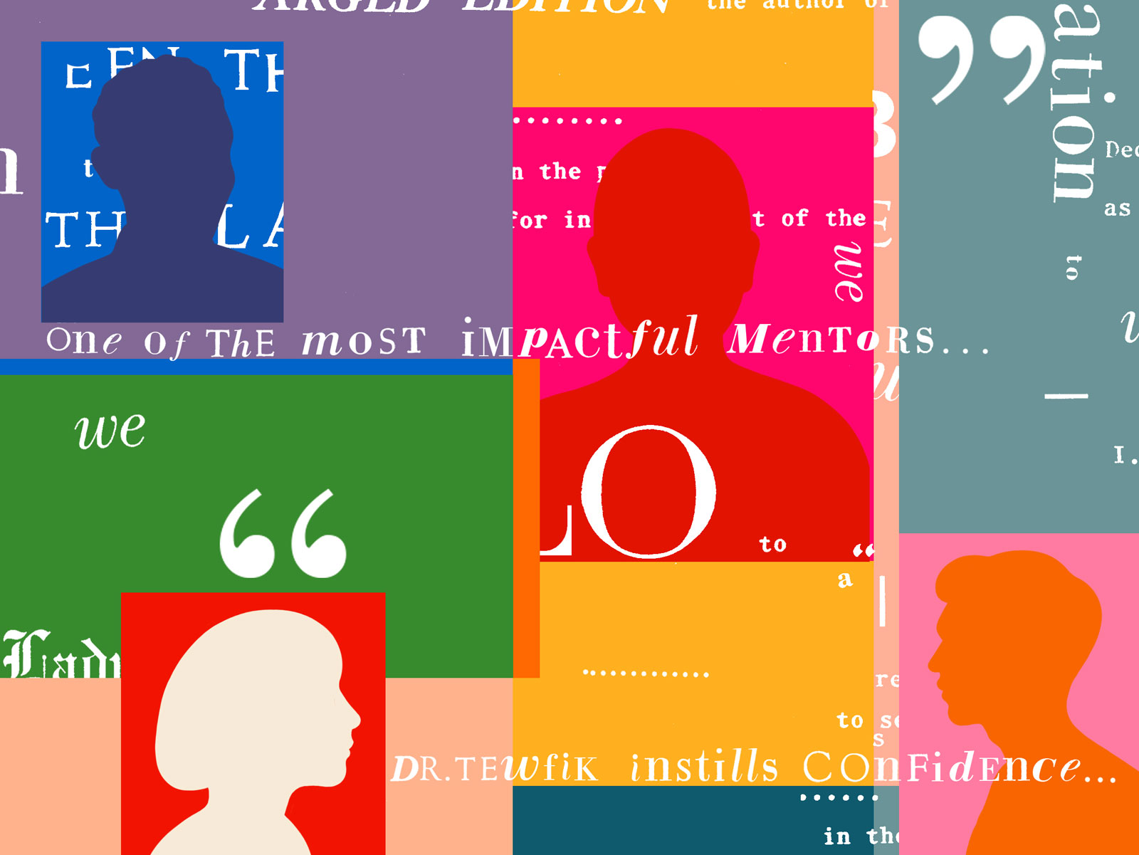
MIT Sloan Professor Relishes Role as a UROP Mentor
Basima Tewfik, who studies impostor syndrome, honored by students for her guidance and commitment to undergraduate research
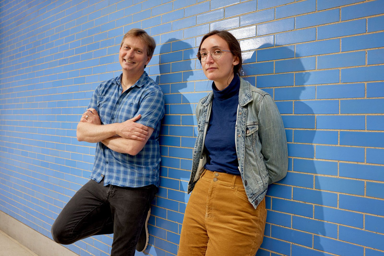
Joey Davis and Laurel Kinman: A Multidimensional Collaboration
Biology professor's support inspires PhD student and protein enthusiast to prioritize mentorship in her career
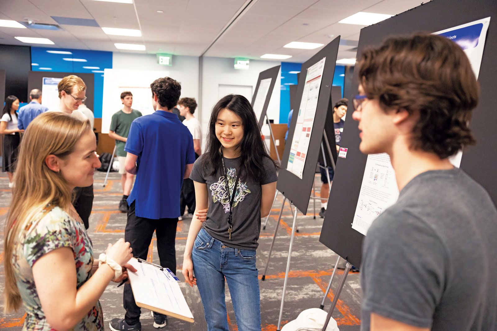
Engineers, Express Yourselves
The MIT School of Engineering Communication Lab, which turned 10 in 2023, helps students translate their work for broader impact
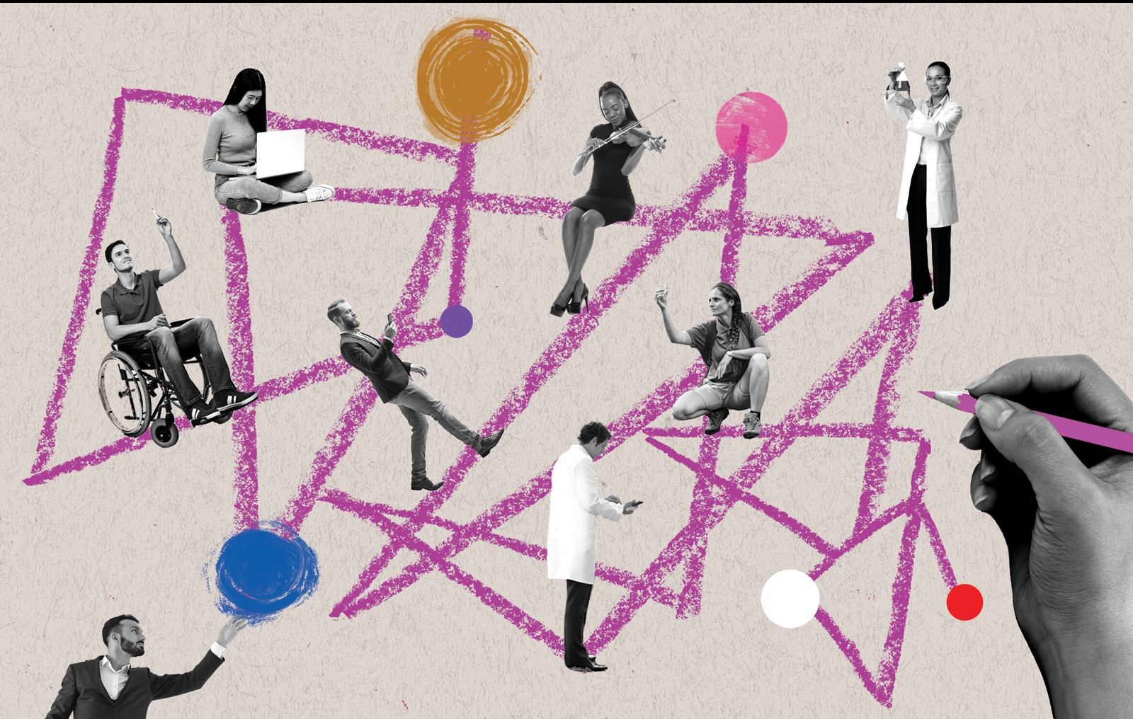
Mentorship in Action Across Campus
MIT's vice president for Resource Development talks about MIT’s robust mentoring landscape and how alumni and friends can play a part
Passing the Baton of Science
Hologic-funded Jay A. Stein Professorship of Biology celebrates MIT innovation across generations
A Trusted Guide Can Make All the Difference
MIT President Sally Kornbluth on mentorship
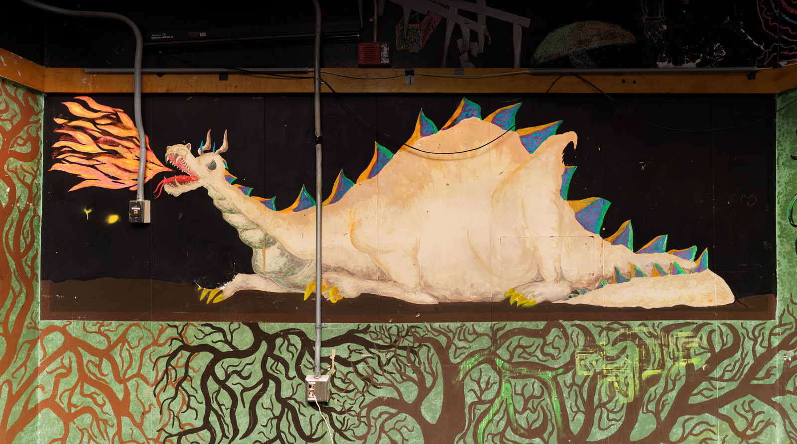
Legacy of Student Art in East Campus
Before East Campus closed in summer 2023 for renovations, a project to digitally preserve some of the most beloved student art got underway
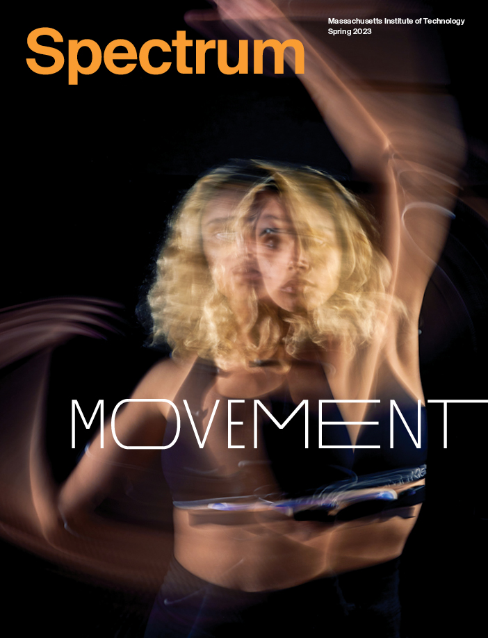
Movement
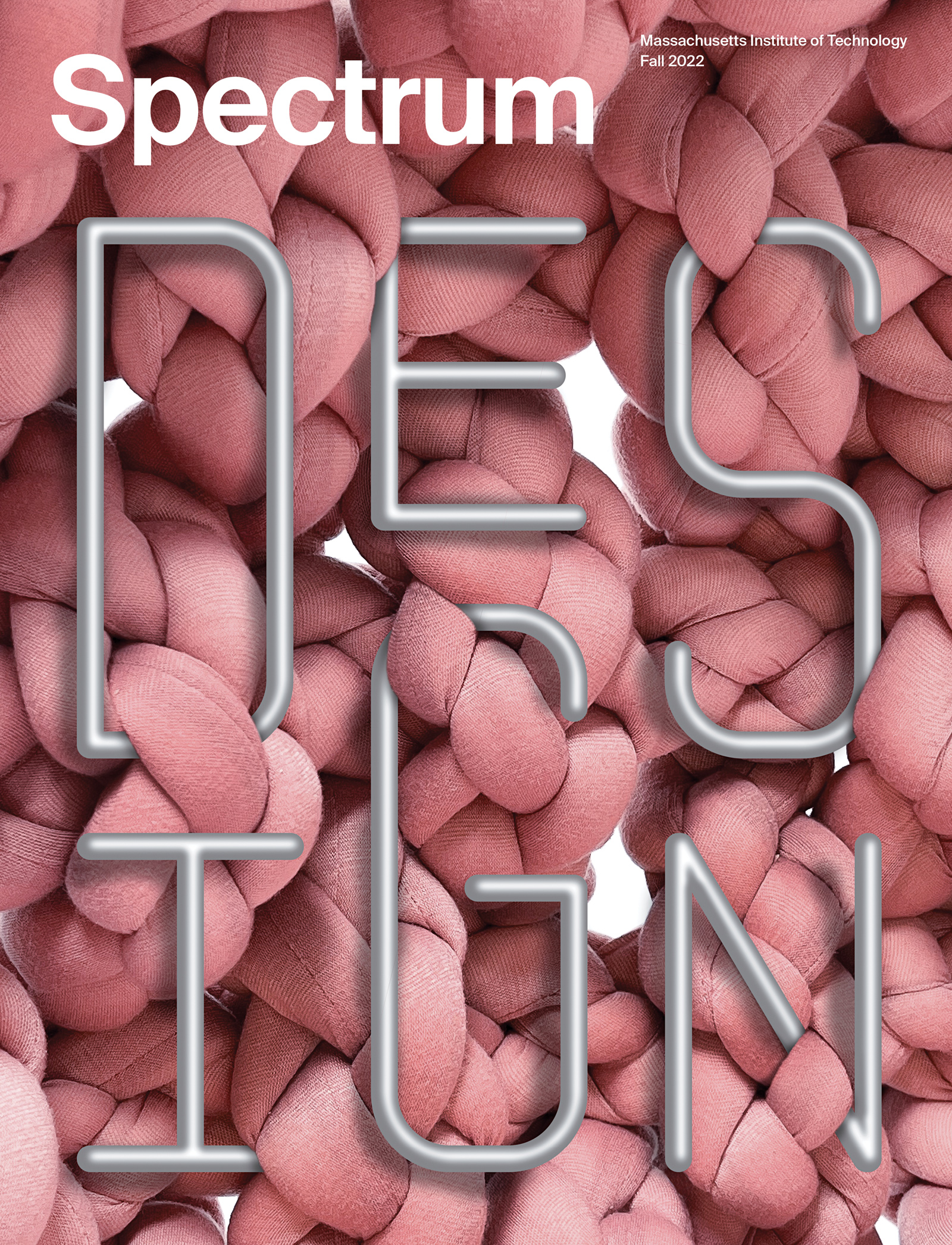
Design

MIT for a Better World

Together

EARTH

Global Health
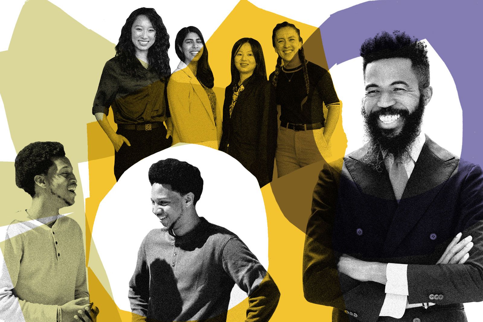
Spotlight On: Mentorship
Your Friendly Neighborhood Mentors at MIT
Resident Peer Mentor program formalizes the peer support that has always been a hallmark of residential culture at the Institute

Designing Effective Applications
MIT graduate architecture students offer guidance to potential applicants from underrepresented groups
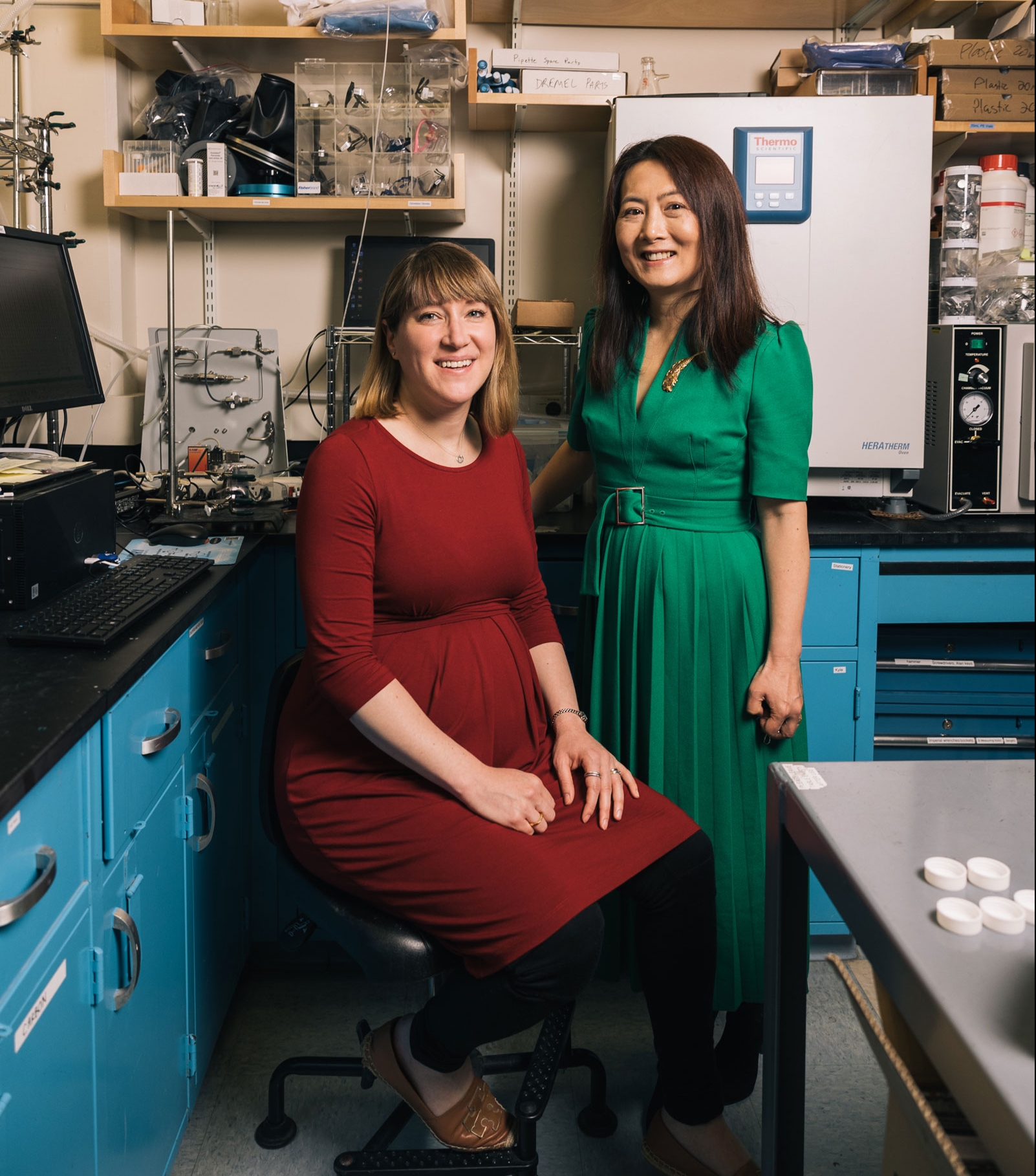
Yang Shao-Horn and Betar Gallant Have Positive Energy
Collaboration with Professor Shao-Horn, who works to uncover materials for next-generation batteries, cultivated Associate Professor Gallant’s intellectual potential
MIT programs provide a mentorship-paved pathway to doctoral degrees—and a potential launch pad to academia
Popular

Two Stories of Philanthropy in the Department of Architecture
Named professorship and significant discretionary funds are “gifts of confidence”
Helping Organizations Learn from Turmoil
Dynamic work design takes a focused approach to tackling challenges
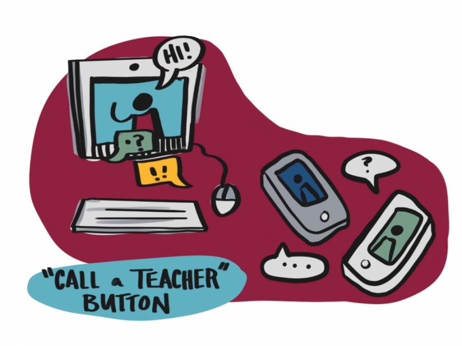
Teaching Lab Steps Up During Pandemic
CMS Professor Justin Reich, colleagues help guide schools in remote learning
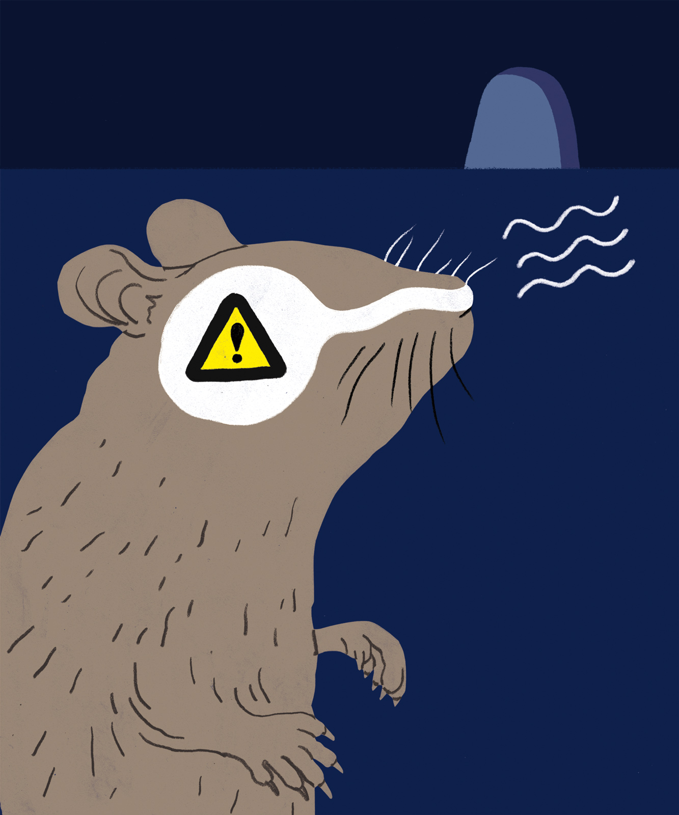
How Does the Brain Connect Smells with Behaviors?
For Gloria Choi, olfactory cues are a gateway to some of the brain’s greatest mysteries